Protein Crystal Manipulation Projects
Microshovels
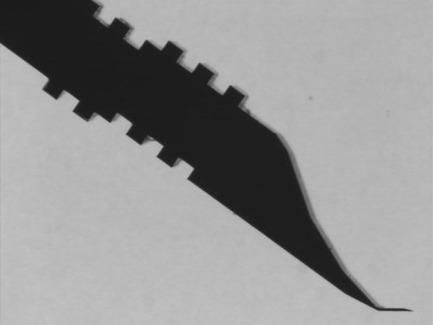
Fig.1: A miscroshovel
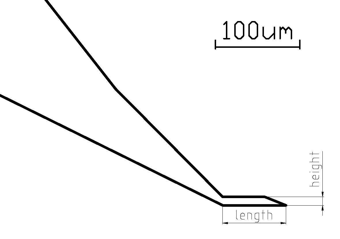
Fig.2: Microshovel tip design
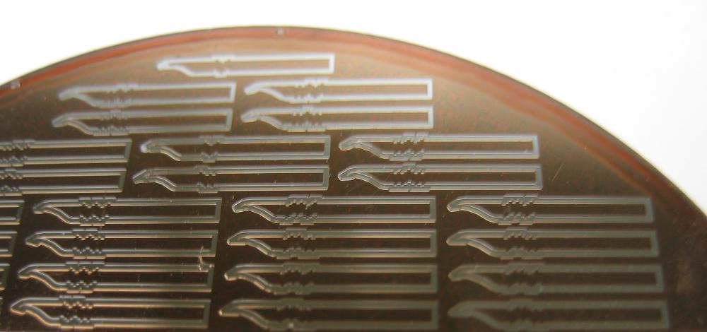
Fig.3: Silicon wafer with microshovels
The microshovels were designed and drawn using the AutoCAD software package (Autodesk). More than 30 different types of microshovels were designed which differed in the shape and the size or their tooltips. The sizes of the fabricated microshovels range from 50 to 280um in length, from 7 to 40um in height, and 300um in width, because these dimensions cover the expected range of protein crystal sizes we would manipulate. The square notches at the bottom of the tool stem encode the shape and the size of the tip so that the microshovels can be easily distinguished by eye or an automatic reading device.
The manufacturing process began with transferring the CAD design onto a 100 x 100mm quartz photomask. Then a front-side photo-lithography was performed on a silicon wafer of 100mm diameter and 300um thickness (which translated to the tool width). The wafer was coated with photoresist, spun in a centrifuge and baked to achieve a uniform coating layer of approximately 10um on each side. One side (the front) was exposed to the pattern from the photomask and developed, while the other side was bonded to a larger sacrificial silicon wafer and the package was processed with deep reactive ion etching (DRIE) leaving the microtools only adherent to the larger wafer. Finally, the microshovels were detached and cleaned up from the bond and the photoresist in an acetone bath.
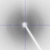
Fig.4: X-ray diffraction patterns

